

MEDIA
Stay Updated with the Latest News from PeiREX.
News
- Admin Hits:12
- 2026-09-28 04:17:30
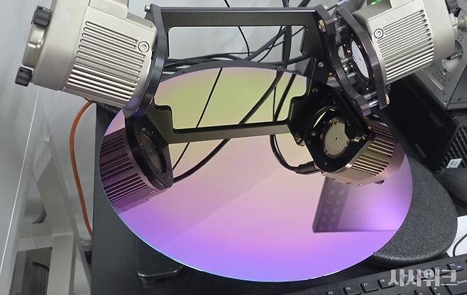
Competition to secure technologies in the ultra-high-density semiconductor market, which dominates the entire AI industry, is intensifying, especially because of the "sensor" technology that can measure plasma conditions in real time.
Sisa Week:
The development of artificial intelligence (AI) is advancing at a remarkable pace, with semiconductors, often referred to as the "brains of AI," playing a central role in this transformation.
According to global management consulting firm McKinsey & Company, the AI semiconductor market is projected to reach $2.3 trillion (approximately KRW 3,121 trillion) by 2030, more than four times South Korea's annual national budget.
As the semiconductor market becomes increasingly critical to the AI industry, competition to secure advanced manufacturing technologies is intensifying. One of the key technologies attracting attention is plasma processing, which plays an essential role in manufacturing ultra-high-density semiconductors.
Plasma processing involves converting semiconductor manufacturing gases, such as halogen-based gases, into a plasma state and precisely controlling the resulting reactions at the atomic scale to create ultrafine semiconductor circuit patterns. Plasma-based processes account for approximately 60–70% of the manufacturing steps involved in producing today's high-performance AI semiconductors.
However, precisely controlling plasma during semiconductor manufacturing is extremely challenging. Plasma conditions can change rapidly depending on process parameters, while directly measuring the plasma state inside processing equipment remains difficult.
These challenges have brought increasing attention to advanced sensor technologies capable of monitoring plasma conditions in real time.
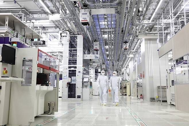
Plasma used in semiconductor and display manufacturing is generated by applying high energy to a gas, causing it to ionize into electrons and positively charged ions. Even slight variations in plasma parameters, such as electron density, electron temperature, ion energy, and ion flux, can significantly affect process outcomes. Plasma sensors detect these variations by monitoring electrical, magnetic, and optical signals.
© Newsis
Ultrafine Semiconductor Processes Drive Growth in the Plasma Diagnostics Market
Plasma used in semiconductor and display manufacturing is generated by applying high energy to a gas, causing it to ionize into electrons and positively charged ions. Plasma is often described as making up approximately 99.9% of the visible matter in the universe and is known as the fourth state of matter, alongside solids, liquids, and gases. In semiconductor manufacturing, plasma is used to facilitate processes such as etching and deposition, enabling the precise removal or addition of material on semiconductor wafer surfaces.
Even slight variations in plasma parameters, such as electron density, electron temperature, ion energy, and ion flux, can significantly affect process outcomes. Plasma sensors detect these variations by monitoring electrical, magnetic, and optical signals. Changes in signal amplitude, frequency, and harmonic components are then analyzed to assess plasma conditions.
Conventional plasma sensors have often been installed directly inside semiconductor processing chambers. However, invasive sensors can interfere with sensitive plasma conditions and potentially affect process stability. To overcome these limitations, advanced non-invasive sensing technologies that monitor signals externally, without direct contact with the plasma, are being actively developed.
In a research paper published in June, researchers at the Korea Institute of Machinery and Materials noted that semiconductor device structures are becoming increasingly complex and process tolerances are becoming more stringent. They emphasized that plasma-based manufacturing requires predictive and adaptive process control capabilities that go beyond conventional experience-based approaches.
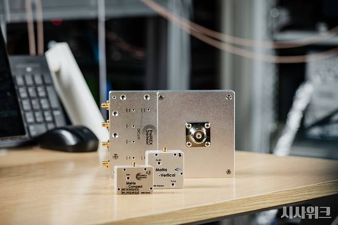
Next-generation plasma sensor developed by PeiREX, a startup specializing in plasma sensing technology. / Photo by Park Sul-min
As plasma monitoring is directly linked to the performance and quality of semiconductor and display manufacturing processes, the market for plasma monitoring technologies has been experiencing rapid growth. According to Semiconductor Insight, a global semiconductor industry market research firm, the plasma process monitoring technology market is projected to reach $139 million (approximately KRW 189 billion) by 2034.
Growth prospects are also strong for the plasma sensor market specifically. According to global market research firm Mobility Foresights, the market is expected to expand from $2.1 billion (approximately KRW 2.85 trillion) in 2025 to $4.9 billion (approximately KRW 6.6 trillion) by 2032, representing a compound annual growth rate (CAGR) of 12.7%.
As the market expands, competition in plasma sensor technology is intensifying internationally. Ireland-based measurement technology company Impedans has commercialized sensors capable of measuring RF voltage, current, and harmonic components to monitor plasma conditions and detect abnormalities in etching processes. Meanwhile, Switzerland-based INFICON provides non-invasive sensing solutions and optical process monitoring technologies for semiconductor manufacturing equipment, enabling external monitoring of plasma-related RF signals.
Mobility Foresights noted that semiconductor technology scaling below the 7 nm node has increased sensitivity to plasma fluctuations, driving greater adoption of advanced sensing technologies. The firm also highlighted that the growing use of advanced packaging processes, along with recurring sensor replacement and calibration requirements, is contributing to sustained market growth.
The Korea Institute of Fusion Energy (KFE) has played a significant role in advancing plasma sensor technology. Selected as the lead institution for a convergence research project funded by the National Research Council of Science and Technology (NST), KFE established the Plasma Equipment Intelligence Research Group in November 2020. The photo shows researchers conducting studies on related technologies. / Photo by Park Sul-min
Reading the Plasma, Not Just the Equipment: Korean Researchers Take on the Challenge
South Korea is accelerating the development of advanced plasma sensor technologies, with the Korea Institute of Fusion Energy (KFE) playing a central role. Selected as the lead institution for a convergence research project under the National Research Council of Science and Technology (NST), KFE established the Plasma Equipment Intelligence Research Group in November 2020. The research group has invested a total of KRW 44 billion in research funding through 2026, developing and demonstrating intelligent technologies for semiconductor plasma processing equipment.
Building on these research achievements, the group established PeiREX, a startup specializing in plasma sensing technology, in January 2026. Leveraging the results of the research program, PeiREX is developing next-generation plasma sensors designed for practical applications in semiconductor and display manufacturing processes.
According to Yoon Jeong-sik, CEO of PeiREX, the company's core technology focuses on detecting changes in radio frequency (RF) signals. In semiconductor and display manufacturing, RF power is used to generate and sustain plasma during processing. An RF-related process failure at a major semiconductor production facility, such as those operated by Samsung Electronics or SK hynix, could potentially result in losses of up to KRW 30 billion per month.
To address these challenges, PeiREX has developed an advanced plasma process diagnostic and optimization sensor by integrating physics-informed artificial intelligence (AI) with conventional plasma sensing technology. When the sensor detects subtle electromagnetic signals from the process chamber, the AI system combines the measured data with physics-based models to estimate critical plasma parameters, including electron temperature, electron density, and ion behavior.
This approach enables semiconductor process engineers to go beyond simply detecting abnormalities and gain deeper insights into their underlying causes, supporting more accurate process diagnostics and optimization.
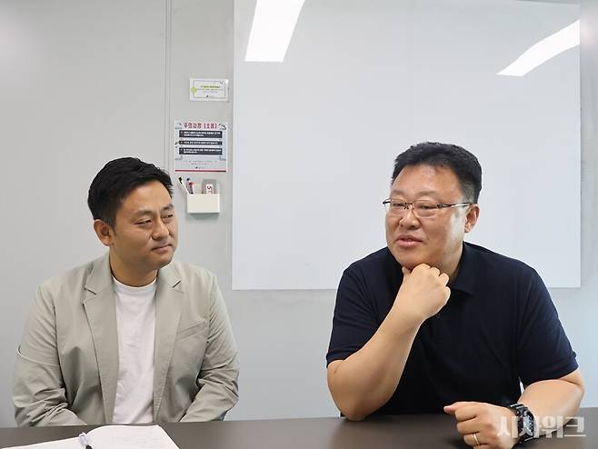
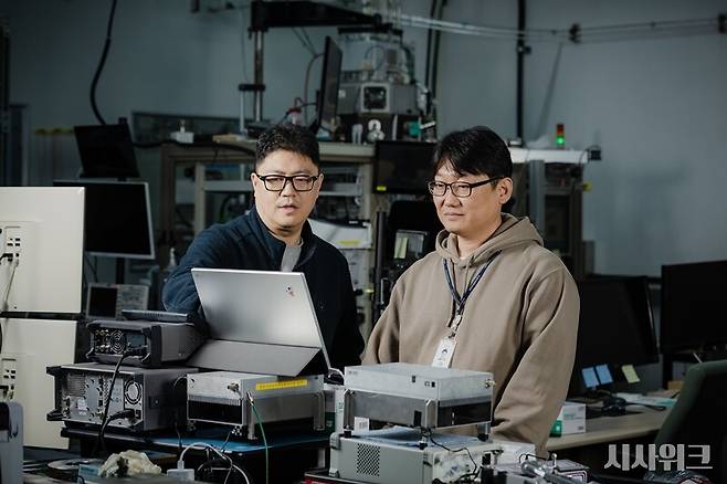
PeiREX's core technology focuses on detecting changes in radio frequency (RF) signals. In semiconductor and display manufacturing processes, RF power is used to generate and sustain plasma. From left: Yoo Woo-jong, CFO of PeiREX, and Yoon Jeong-sik, CEO of PeiREX and Head of the Plasma Equipment Intelligence Research Group at the Korea Institute of Fusion Energy (KFE). / Photo by Park Sul-min
According to PeiREX, its technology is currently undergoing validation on an 8.6-generation production line operated by a domestic display manufacturer, with potential expansion to hundreds of plasma etching systems.
"Conventional AI relies on large volumes of data to identify patterns and predict outcomes. However, plasma sensing requires AI that can explain the underlying causes by incorporating physics-based models," said Yoon Jeong-sik, Head of the Plasma Equipment Intelligence Research Group. "The semiconductor and display industries now need technologies that go beyond simply detecting abnormalities to explain why specific process outcomes occur."
"RF signals, once regarded as mere noise, actually contain valuable information about plasma conditions and manufacturing processes," he added. "The key to PeiREX's technology lies in analyzing these signals to identify the unique 'fingerprints' of equipment and process conditions."
Yoo Woo-jong, CFO of PeiREX, stated, "PeiREX was established based on technologies developed through approximately five years of government-funded R&D and industrial field demonstrations conducted by the Plasma Equipment Intelligence Research Group since 2020." He added, "Our technological competitiveness is supported by research achievements from national R&D programs and technology validation conducted in collaboration with major industry partners."
Copyright © Sisaweek. All rights reserved. Unauthorized reproduction and redistribution are prohibited.
☞ View Original Article https://v.daum.net/v/20260928173021134

PeiREX Co., Ltd.
Business Registration Number 474-86-03949
CEO Yoon Jeong-sik
99, Daehak-ro, Yuseong-gu, Daejeon, Republic of Korea 409, Daehak-ro, Yuseong-gu, Daejeon (Gung-dong, Chungnam National University)
Email. contact@peirex.co.kr
